This circuit produces bright flashes every second or so. R1 controls flash rate. L1 can replace with 3V or 4.5V flash light or for simply you can use a LED for example.
May 21, 2011
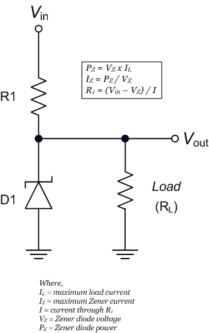
Zener Voltage Regulator
This circuit supplies a steady voltage (Vout) to a load from an unregulated supply (like a battery), Vin can vary but must be at least 1 volt above desired Vout. I, can vary from 0 mA to planned maximum value. I does not change if IL falls to 0 mA. Since I = IL + IZ, IZ rises as IL falls. In other words, the regulator always uses the same current, even when the load is removed. Caution: D1 and R1 must have proper power rating. Use Ohm's Law.
Example:
A radio draws from 20 to 50 mA from a 9 volt battery. To power it from a 12 volt batery, use a 9 volt, 1/2 watt Zener Diode. R1 should be closed to 60 ohm and rated for at least 0.15 W.
Labels:
Projects
Voltage Doublers
These circuit approximately double an incoming AC voltage. The output is DC. Use capacitors and diodes rated for twice the input voltage. Output ripple can be reduced by using large values for C1 and C2.
Labels:
Projects
May 16, 2011
Fritzing (Electronics Software)
Fritzing is an open source GUI based program that allows users to document their prototypes, share them with others, show them in a presentation, and create a pcb layout for professional manufacturing. This is the latest version of Fritzing that released till today (version 0.5.2b). You can check for the Fritzing update directly on the Help tab on Fritzing window.
Download Fritzing 0.5.2b
Here's I give a quick tutorial using fritzing so it can help you to understand how to use fritzing more easily, have fun! :-)
Labels:
Software
April 17, 2011
Binary Subtraction
Half subtractors and full subtractors will be explained in this section. The rules for the binary subtraction of two bits are given in Fig. 1. The top number in a subtraction problem is called the minuend. The bottom number is called the subtrahend, and the answer is called the difference. Rule 1 in Fig. 1 is obvious. Rule 2 (Fig. 1) concerns 1 being subtracted from the smaller number 0. In Fig. 2, note that, in the Is column of the binary number, 1 is subtracted from 0. A 1 must be borrowed from the binary 2s column, leaving a 0 in that column. Now the subtrahend 1 is subtracted from the minuend 10 (decimal 2). This leaves a difference of 1 in the Is column. The binary 2s column uses rule 1 (0-0) and is equal to 0. Therefore, rule 2 is 0 - 1 = 1 with a borrow of 1. Rules 3 and 4 are also rather obvious.
The subtraction rules given in Fig. 1 look somewhat like a truth table. These rules have been reproduced in truth table form in Fig. 3. Consider the difference (Di) output in the truth table. Note that this output represents the XOR function. The logic function for the difference output in a subtractor is the same as that for the sum output in a half adder circuit. Now consider the borrow (Bo) column in the truth table. The logic function for this column can be represented by the Boolean expression A’ • B = Y. It can be implemented by using an inverter and a 2-input AND gate.
The truth table in Fig. 3 represents a logic circuit called a half subtractor. The Boolean expression for the difference output is A(xor)B = Di. The Boolean expression for the borrow (Bo) output is A’ • B = Bo. A half subtractor would be wired from logic gates as shown in Fig. 4a. Input A is the minuend and B is the subtrahend. The Di output is the difference; Bo is the borrow. A simplified block diagram for a half subtractor is in Fig. 4b.
Compare the half subtractor logic diagram in Fig. 4a with the half adder (in figure in the previous post). The only difference in the logic circuits is that the half subtractor has one added inverter at the A input of the AND gate.
Consider the subtraction problem in Fig. 5. Several borrows are evident in this problem. If six subtractor circuits are used for the six binary places, the borrows must be considered. A half subtractor may be used for the Is place. Full subtractors must be used in the 2s. 4s. 8s. 16s. and 32s columns of this problem.
A block diagram of a full subtractor (FS) is in Fig. 6. The inputs are A (minuend). B (subtrahend), and Bin (borrow input). The outputs are Di (difference) and Bo (borrow output). The Bo and Bin lines are connected from subtractor to subtractor to keep track of the borrows.
The diagram in Fig. 6b shows how to wire two half subtractors (HS) and an OR gate together to form a full subtractor (FS) circuit. Note that the wiring pattern is similar to that used for adders. Finally, Fig. 7 shows how gates could be wired to form a full subtractor circuit. Remember that full subtractors must be used to subtract all columns except the Is column in binary subtraction.
The truth table for the full subtractor is in Fig. 8. The inputs are labeled as minuend (A), subtrahend (B), and borrow in (Bin). The outputs are the customary difference (Di) and borrow out (Bo).
The binary subtraction problem in Fig. 9 will aid understanding of the full subtractor truth table. Follow as this problem is solved, using only the truth tables in Figs. 3 and 8. Look at the Is column of the problem in Fig. 9. The Is place uses a half subtractor. Find this situation in the truth table in Fig. 3. You find that line 3 of the half subtractor truth table gives an output of 1 for Di (difference) and 0 for borrow out (Bo). This is recorded below the Is column in Fig. 9.
Consider the 2s column in Fig. 9. The 2s column uses a full subtractor. On the full subtractor truth table, look for the situation where A = 0, B = 0, and Bin = 0. This is line 1 in Fig. 8. According to the truth table, both outputs (Di and Bo) are 0. This is recorded below the 2s column in Fig. 9.
Next consider the 4s column in Fig. 9. The inputs to this full subtractor will be A = 1, B = 1, and Bin = 0. Looking at the input side of the truth table in Fig. 8, it appears that line 7 shows this situation. The outputs (Di and Bo) are both 0 according to the truth table and are written as such on Fig. 9 under the 4s column.
Look at the 8s column in Fig. 9. The inputs to the full subtractor will be A = 0, B = 1, and Bin = 0. Line 3 of the truth table (Fig. 8) shows this situation. The outputs (Di and Bo) in line 3 are both Is and are recorded in the 8s column in Fig. 9.
The 16s column in Fig. 9 has inputs of A = 1, B = 1, and Bin = 1. This corresponds with line 8 in the truth table. Line 8 generates an output of Di = 1 and Bo = 1. These Is are recorded under the 16s column in the problem.
The 32s column has inputs of A = 1, B = 0, and Bin = 1. This corresponds to line 6 in the truth table in Fig. 8. Line 6 generates outputs of Di = 0 and Bo = 0. These 0s are recorded in the 32s column of the problem.
Finally consider the 64s column in Fig. 9. The inputs to the full subtractor are A = 1, B = 0, and Bin = 0. This input combination is shown in line 5 in the truth table. Line 5 generates an output of Di = 1 and Bo = 0. Figure 9 illustrates how binary 11100 is subtracted from binary 1110101 using truth tables. The borrows are shown below the problem. This procedure is quite cumbersome for humans, but electronic circuits can accurately perform this subtraction in microseconds.
Labels:
Digital Electronics
Binary Addition
Adding binary numbers is a very simple task. The rules (addition tables) for binary addition using two bits are shown in Fig. 8-1. The first three rules are obvious. Rule 4 says that, in binary, 1 + 1 = 10 (decimal 2). The 1 in the sum must be carried to the next column as in regular decimal addition.
Two sample binary addition problems are shown below:
It is now possible to design a gating circuit that will perform addition. Looking at the left two columns of Fig.1 reminds one of a two-variable truth table. The binary rules are reproduced in truth table form in Fig. 3. The inputs to be added are given the letters A and B. The sum output is often given the summation symbol (∑). The carry-out output column is often just represented with the Co symbol.
The truth table in Fig. 3 is that of a half adder circuit. A block diagram for a half adder might be drawn as in Fig. 4a. Note the two inputs A and B on the symbol in Fig. 4a. The outputs are labeled ∑ (sum) and Co (carry out). It is common to label the half adder with HA as shown on the block symbol.
Looking at the sum (∑) output column of the truth table in Fig. 3, note that it takes an XOR function to produce the ∑ output. The carry-out column will use an AND function. A complete logic circuit for the half adder with two inputs (A and B) and two outputs (∑ and Co) is shown in Fig. 4b. Composed only of gates (XOR and AND), the half adder is classified as a combinational logic circuit.
Consider the binary addition problem in Fig. 5a. The Is column is 1 + 1, and it follows rule 4 in Fig. 1. The sum is 0 with a carry of 1 to the 2s column. The 2s column must now be added. In the 2s column we have 1 + 1 + 1. This is a new situation. It equals binary 11 (decimal 3). The 1 is placed below the 2s column in the sum position. A 1 is carried to the 4s column. The single 1 at the top of the 4s column is added to the Os with a result of 1, which is written in the sum position. The result is a sum of 110.
Rule 5 for binary addition is formally written in Fig. 4/5. Note the three inputs (A, B, and carry in). The outputs are the usual sum and carry out. Rule 5 suggests that a half adder will not work if a carry-in situation arises. Half adders will add only two inputs (A and B), as in the Is column of an addition problem. When the 2s column or the 4s column is added, a new circuit is needed. The new circuit is called a full adder. A block diagram of a full adder is shown in Fig. 6a.
The full adder circuit has three inputs which are added. The inputs shown in the block diagram in Fig. 6 are A, B, and On (carry in). The outputs from the full adder are the customary ∑ (sum) and Co (carry out). Note the use of the letters FA to symbolize full adder in the block diagram. To repeat, the half adder is used in only the Is place when larger binary numbers are added. Full adders are used for adding all other columns (2s, 4s, 8s, and so forth).
A full adder circuit can be constructed from half adders and an OR gate. A full adder circuit is diagrammed in Fig. 6b. The half adder becomes a basic building block in constructing other adders. A truth table for the full adder is detailed in Fig. 7.
Labels:
Digital Electronics
April 16, 2011
Combinational Logic Circuit
Multiple gate functions can be combined to form more complex or different Boolean logic functions. Wiring together multiple gates are used to build a complex logic function that only outputs a specific value when a specific combination of True and False inputs are passed to it is known as ‘‘combinatorial logic’’. The output of a combinatorial logic circuit is dependent on its input; if the input changes then the output will change as well.
When I wrote the preceding paragraph, I originally noted that combinatorial logic circuits produce a ‘‘True’’ output for a given set of inputs. This is incorrect, as there will be some cases where you will require a False output in your application. I made the definition a bit more ambiguous so that you do not feel like the output has to be a single, specific value when the input consists of the required inputs. It is also important to note that in a combinatorial logic circuit, data flows in one direction and outputs in logic gates cannot be used as inputs to gates which output back to themselves. These two points may seem subtle now, but they are actually critically important to the definition of combinatorial logic circuits and using them in applications.
An example of a combinatorial circuit is shown in figure above. In this circuit, I have combined three AND gates, a NOR gate, a NOT gate and an XOR gate to produce the following logic function:
This combinatorial circuit follows the convention that inputs to a gate (or a chip or other electronic component) are passed into the left and outputs exit from the right. This will help you ‘‘read’’ the circuit from left to right, something that should be familiar to you.
While seeing a series of logic gates, like the one in figure above seems to be overwhelming, you already have the tools to be able to work through it and understand how it works. In the previous section, I noted that gates could be connected by passing the output of one into an input of another; a combinatorial circuit (like figure) is simply an extension of this concept and, being an extension, you can use the same tools you used to understand single gates to understand the multiple gate operation.
Labels:
Digital Electronics
Logic Gates
Various forms of logical building blocks are available in integrated circuit form. These logical building blocks are called “gates,” with each gate having a distinct function. Logic gates can be further combined into more complex digital building blocks to perform a variety of counting, memory, and timing functions.
Digital ICs are grouped into families, with each family possessing certain desirable traits that make them more or less suited to a variety of applications. One logic family might not be compatible with another family, so it is typical for the designer to use only one family type for each application. The most commonly used logic families in the present market are complementary metal oxide silicon (CMOS) and transistor-transistor logic (TTL).
Logic gates respond to “high” or “low” voltage levels. The specific voltage level for a “high” or “low” condition will vary from one logic family to another. For example, a logical one (high) in TTL logic is about 5 volts; in contrast, a possible 12-volt level might be used for CMOS logic. However, the functional operation and symbolic representation is universal throughout all of the families. In figure below lists some of the more common logic devices and their associated symbols.
Logic gates, and other logic devices, are functionally defined by using truth tables. The second figure illustrates a variety of truth tables for some common logic gates. Compare the AND-gate illustration in first figure with its corresponding truth table in second figure. Because the AND gate has two input leads, there are a total of four possible logic conditions that could occur on the inputs. Notice that the truth table lists the four possible input conditions; together with each of their resultant outputs for each condition. As shown by the truth table, the only time that the output goes “high” is when the A input “and” the B input are high.
Logic gates can have more than two inputs. Second figure illustrates the truth table for a three-input AND gate. Common logic gates are available with up to eight inputs.
Referring again to first figure, note the OR gate and its associated truth table in second figure. As the name implies, its output goes high whenever a high appears on the A input, or on the B input (or both).
In digital terminology, a not function means that a logical condition is inverted, or reversed. A NAND gate (short for not AND) is an AND gate, with the output inverted. Notice that the outputs in the truth tables for the AND gate, and the NAND gate, are simply inverted. This same principle holds true for the OR and NOR gates.
It is common for the output of one logic gate to provide inputs for several other logic gates. The maximum number of inputs that can be driven by a particular logic gate is specified as its fanout. Typical logic gates have fanouts ranging from 5 to 20. If it becomes necessary to drive a greater number of inputs than the fanout of a particular gate, a buffer is used to increase the fanout capability. The symbol for a buffer is illustrated in first figure.
The need often arises to invert a logic signal. The symbol for an inverter is shown in first figure. An inverter is sometimes called a not gate. Note that it has a small circle on its output just like the NOT AND (NAND) and NOT OR (NOR) gates. Anytime a small circle appears on an input or output of a logic device, it is symbolizing the inversion of the logic signals (or data). Also notice the horizontal line above the A output of the inverter. It is called a not symbol. Whenever a horizontal line is placed above a logic expression, it means that it is inverted.
Another common type of logic gate is the exclusive OR gate. Refer to its symbol and the associated truth table in first and second figures. As the truth table indicates, its output only goes high when its inputs are different from each other. The exclusive NOR gate provides the same logic function with an inverted output.
Labels:
Digital Electronics
Subscribe to:
Posts (Atom)