Pages

April 17, 2011

Binary Subtraction


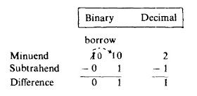
          Half subtractors and full subtractors will be explained in this section. The rules for the binary subtraction of two bits are given in Fig. 1. The top number in a subtraction problem is called the minuend. The bottom number is called the subtrahend, and the answer is called the difference. Rule 1 in Fig. 1 is obvious. Rule 2 (Fig. 1) concerns 1 being subtracted from the smaller number 0. In Fig. 2, note that, in the Is column of the binary number, 1 is subtracted from 0. A 1 must be borrowed from the binary 2s column, leaving a 0 in that column. Now the subtrahend 1 is subtracted from the minuend 10 (decimal 2). This leaves a difference of 1 in the Is column. The binary 2s column uses rule 1 (0-0) and is equal to 0. Therefore, rule 2 is 0 - 1 = 1 with a borrow of 1. Rules 3 and 4 are also rather obvious.


          The subtraction rules given in Fig. 1  look somewhat like a truth table. These rules have been reproduced in truth table form in Fig. 3. Consider the difference (Di) output in the truth table. Note that this output represents the XOR function. The logic function for the difference output in a subtractor is the same as that for the sum output in a half adder circuit. Now consider the borrow (Bo) column in the truth table. The logic function for this column can be represented by the Boolean expression A’ • B = Y. It can be implemented by using an inverter and a 2-input AND gate.


          The truth table in Fig. 3 represents a logic circuit called a half subtractor. The Boolean expression for the difference output is A(xor)B = Di. The Boolean expression for the borrow (Bo) output is A’ • B = Bo. A half subtractor would be wired from logic gates as shown in Fig. 4a. Input A is the minuend and B is the subtrahend. The Di output is the difference; Bo is the borrow. A simplified block diagram for a half subtractor is in Fig. 4b.

          Compare the half subtractor logic diagram in Fig. 4a with the half adder (in figure in the previous post). The only difference in the logic circuits is that the half subtractor has one added inverter at the A input of the AND gate.
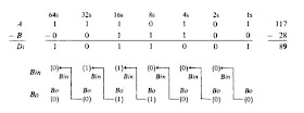
          Consider the subtraction problem in Fig. 5. Several borrows are evident in this problem. If six subtractor circuits are used for the six binary places, the borrows must be considered. A half subtractor may be used for the Is place. Full subtractors must be used in the 2s. 4s. 8s. 16s. and 32s columns of this problem.


          A block diagram of a full subtractor (FS) is in Fig. 6. The inputs are A (minuend). B (subtrahend), and Bin (borrow input). The outputs are Di (difference) and Bo (borrow output). The Bo and Bin lines are connected from subtractor to subtractor to keep track of the borrows.


          The diagram in Fig. 6b shows how to wire two half subtractors (HS) and an OR gate together to form a full subtractor (FS) circuit. Note that the wiring pattern is similar to that used for adders. Finally, Fig. 7 shows how gates could be wired to form a full subtractor circuit. Remember that full subtractors must be used to subtract all columns except the Is column in binary subtraction. 
          The truth table for the full subtractor is in Fig. 8. The inputs are labeled as minuend (A), subtrahend (B), and borrow in (Bin). The outputs are the customary difference (Di) and borrow out (Bo).


          The binary subtraction problem in Fig. 9 will aid understanding of the full subtractor truth table. Follow as this problem is solved, using only the truth tables in Figs. 3 and 8. Look at the Is column of the problem in Fig. 9. The Is place uses a half subtractor. Find this situation in the truth table in Fig. 3. You find that line 3 of the half subtractor truth table gives an output of 1 for Di (difference) and 0 for borrow out (Bo). This is recorded below the Is column in Fig. 9.


          Consider the 2s column in Fig. 9. The 2s column uses a full subtractor. On the full subtractor truth table, look for the situation where A = 0, B = 0, and Bin = 0. This is line 1 in Fig. 8. According to the truth table, both outputs (Di and Bo) are 0. This is recorded below the 2s column in Fig. 9.
          Next consider the 4s column in Fig. 9. The inputs to this full subtractor will be A = 1, B = 1, and Bin = 0. Looking at the input side of the truth table in Fig. 8, it appears that line 7 shows this situation. The outputs (Di and Bo) are both 0 according to the truth table and are written as such on Fig. 9 under the 4s column.
          Look at the 8s column in Fig. 9. The inputs to the full subtractor will be A = 0, B = 1, and Bin = 0. Line 3 of the truth table (Fig. 8) shows this situation. The outputs (Di and Bo) in line 3 are both Is and are recorded in the 8s column in Fig. 9. 
          The 16s column in Fig. 9 has inputs of A = 1, B = 1, and Bin = 1. This corresponds with line 8 in the truth table. Line 8 generates an output of Di = 1 and Bo = 1. These Is are recorded under the 16s column in the problem.   
          The 32s column has inputs of A = 1, B = 0, and Bin = 1. This corresponds to line 6 in the truth table in Fig. 8. Line 6 generates outputs of Di = 0 and Bo = 0. These 0s are recorded in the 32s column of the problem. 
          Finally consider the 64s column in Fig. 9. The inputs to the full subtractor are A = 1, B = 0, and Bin = 0. This input combination is shown in line 5 in the truth table. Line 5 generates an output of Di = 1 and Bo = 0. Figure 9 illustrates how binary 11100 is subtracted from binary 1110101 using truth tables. The borrows are shown below the problem. This procedure is quite cumbersome for humans, but electronic circuits can accurately perform this subtraction in microseconds.



Binary Addition


          Adding binary numbers is a very simple task. The rules (addition tables) for binary addition using  two bits are shown in Fig. 8-1. The first three rules are obvious. Rule 4 says that, in binary, 1 + 1 = 10  (decimal 2). The 1 in the sum must be carried to the next column as in regular decimal addition.


Two sample binary addition problems are shown below:


          It is now possible to design a gating circuit that will perform addition. Looking at the left two columns of Fig.1 reminds one of a two-variable truth table. The binary rules are reproduced in truth table form in Fig. 3. The inputs to be added are given the letters A and B. The sum output is often given the summation symbol (∑). The carry-out output column is often just represented with the Co symbol.


          The truth table in Fig. 3 is that of a half adder circuit. A block diagram for a half adder might be drawn as in Fig. 4a. Note the two inputs A and B on the symbol in Fig. 4a. The outputs are labeled ∑ (sum) and Co (carry out). It is common to label the half adder with HA as shown on the block symbol.


          Looking at the sum (∑) output column of the truth table in Fig. 3, note that it takes an XOR function to produce the ∑ output. The carry-out column will use an AND function. A complete logic circuit for the half adder with two inputs (A and B) and two outputs (∑ and Co) is shown in Fig. 4b. Composed only of gates (XOR and AND), the half adder is classified as a combinational logic circuit.
          Consider the binary addition problem in Fig. 5a. The Is column is 1 + 1, and it follows rule 4 in Fig. 1. The sum is 0 with a carry of 1 to the 2s column. The 2s column must now be added. In the 2s column we have 1 + 1 + 1. This is a new situation. It equals binary 11 (decimal 3). The 1 is placed below the 2s column in the sum position. A 1 is carried to the 4s column. The single 1 at the top of the 4s column is added to the Os with a result of 1, which is written in the sum position. The result is a sum of 110.


          Rule 5 for binary addition is formally written in Fig. 4/5. Note the three inputs (A, B, and carry in). The outputs are the usual sum and carry out. Rule 5 suggests that a half adder will not work if a carry-in situation arises. Half adders will add only two inputs (A and B), as in the Is column of an addition problem. When the 2s column or the 4s column is added, a new circuit is needed. The new circuit is called a full adder. A block diagram of a full adder is shown in Fig. 6a.


          The full adder circuit has three inputs which are added. The inputs shown in the block diagram in Fig. 6 are A, B, and On (carry in). The outputs from the full adder are the customary ∑ (sum) and Co (carry out). Note the use of the letters FA to symbolize full adder in the block diagram. To repeat, the half adder is used in only the Is place when larger binary numbers are added. Full adders are used for adding all other columns (2s, 4s, 8s, and so forth).
          A full adder circuit can be constructed from half adders and an OR gate. A full adder circuit is diagrammed in Fig. 6b. The half adder becomes a basic building block in constructing other adders. A truth table for the full adder is detailed in Fig. 7.


April 16, 2011

Combinational Logic Circuit


          Multiple gate functions can be combined to form more complex or different Boolean logic functions. Wiring together multiple gates are used to build a complex logic function that only outputs a specific value when a specific combination of True and False inputs are passed to it is known as ‘‘combinatorial logic’’. The output of a combinatorial logic circuit is dependent on its input; if the input changes then the output will change as well.
          When I wrote the preceding paragraph, I originally noted that combinatorial logic circuits produce a ‘‘True’’ output for a given set of inputs. This is incorrect, as there will be some cases where you will require a False output in your application. I made the definition a bit more ambiguous so that you do not feel like the output has to be a single, specific value when the input consists of the required inputs. It is also important to note that in a combinatorial logic circuit, data flows in one direction and outputs in logic gates cannot be used as inputs to gates which output back to themselves. These two points may seem subtle now, but they are actually critically important to the definition of combinatorial logic circuits and using them in applications. 


          An example of a combinatorial circuit is shown in figure above. In this circuit, I have combined three AND gates, a NOR gate, a NOT gate and an XOR gate to produce the following logic function:


 This combinatorial circuit follows the convention that inputs to a gate (or a chip or other electronic component) are passed into the left and outputs exit from the right. This will help you ‘‘read’’ the circuit from left to right, something that should be familiar to you.
          While seeing a series of logic gates, like the one in figure above seems to be overwhelming, you already have the tools to be able to work through it and understand how it works. In the previous section, I noted that gates could be connected by passing the output of one into an input of another; a combinatorial circuit (like figure) is simply an extension of this concept and, being an extension, you can use the same tools you used to understand single gates to understand the multiple gate operation.


Logic Gates


          Various forms of logical building blocks are available in integrated circuit form. These logical building blocks are called “gates,” with each gate having a distinct function. Logic gates can be further combined into more complex digital building blocks to perform a variety of counting, memory, and timing functions. 
          Digital ICs are grouped into families, with each family possessing certain desirable traits that make them more or less suited to a variety of applications. One logic family might not be compatible with another family, so it is typical for the designer to use only one family type for each application. The most commonly used logic families in the present market are complementary metal oxide silicon (CMOS) and transistor-transistor logic (TTL). 
          Logic gates respond to “high” or “low” voltage levels. The specific voltage level for a “high” or “low” condition will vary from one logic family to another. For example, a logical one (high) in TTL logic is about 5 volts; in contrast, a possible 12-volt level might be used for CMOS logic. However, the functional operation and symbolic representation is universal throughout all of the families. In figure below lists some of the more common logic devices and their associated symbols. 


          Logic gates, and other logic devices, are functionally defined by using truth tables. The second figure illustrates a variety of truth tables for some common logic gates. Compare the AND-gate illustration in first figure with its corresponding truth table in second figure. Because the AND gate has two input leads, there are a total of four possible logic conditions that could occur on the inputs. Notice that the truth table lists the four possible input conditions; together with each of their resultant outputs for each condition. As shown by the truth table, the only time that the output goes “high” is when the A input “and” the B input are high. 
          Logic gates can have more than two inputs. Second figure illustrates the truth table for a three-input AND gate. Common logic gates are available with up to eight inputs. 
Referring again to first figure, note the OR gate and its associated truth table in second figure. As the name implies, its output goes high whenever a high appears on the A input, or on the B input (or both). 
In digital terminology, a not function means that a logical condition is inverted, or reversed. A NAND gate (short for not AND) is an AND gate, with the output inverted. Notice that the outputs in the truth tables for the AND gate, and the NAND gate, are simply inverted. This same principle holds true for the OR and NOR gates. 
          It is common for the output of one logic gate to provide inputs for several other logic gates. The maximum number of inputs that can be driven by a particular logic gate is specified as its fanout. Typical logic gates have fanouts ranging from 5 to 20. If it becomes necessary to drive a greater number of inputs than the fanout of a particular gate, a buffer is used to increase the fanout capability. The symbol for a buffer is illustrated in first figure. 
          The need often arises to invert a logic signal. The symbol for an inverter is shown in first figure. An inverter is sometimes called a not gate. Note that it has a small circle on its output just like the NOT AND (NAND) and NOT OR (NOR) gates. Anytime a small circle appears on an input or output of a logic device, it is symbolizing the inversion of the logic signals (or data). Also notice the horizontal line above the A output of the inverter. It is called a not symbol. Whenever a horizontal line is placed above a logic expression, it means that it is inverted. 
          Another common type of logic gate is the exclusive OR gate. Refer to its symbol and the associated truth table in first and second figures. As the truth table indicates, its output only goes high when its inputs are different from each other. The exclusive NOR gate provides the same logic function with an inverted output.


Introduction to Digital Electronics


Digital electronics is a large branch of the electrical-electronics field relating to those electronic functions used in performing logical functions. It encompasses every type of logical system from simple combinational logic control in a coffee pot to the largest computer systems. The concept of digital control is not new. Even before the first computer appeared, or solid-state electronics came into being, large banks of relays were performing logical control functions in industrial facilities.


          The earliest types of computers were called analog computers. They were enormous machines made from thousands of vacuum tubes. Computations were performed using voltage levels based on the decimal (base 10) numbering system. Although this method seems natural because you think in terms of tens (because you were created with 10 fingers), the old analog computers soon gave way to the more modern binary computers (base 2). There are very good reasons for this change, which will be explained as this chapter continues. 
          Although many people seem to have trouble comprehending different numbering systems, it’s really quite simple. The key is in understanding the mechanics behind the decimal system, and then applying those principles to any other numbering system. 
          The term decimal means “base 10.” If the number 1543 is broken down into decimal column weights, it comes out to 3 units (or ones), 4 tens, 5 hundreds, and 1 thousand. Notice how each succeeding weight is actually the base number (10) times the “weight” of the preceding column. In other words, 1 x 10 = 10, 10 x 10 = 100, 10 x 100 = 1000, and so on. 
          The binary numbering system works exactly the same way, except that it is based on 2 instead of 10. For example, the first weight (or least significant digit) is the units, or ones, column. The weight of the second column is 2 x 1, or 2. The next column is 2 x 2, or 4. The next column is 2 x 4, or 8. Instead of the column weights being ones, tens, hundreds, thousands, ten thousands, and so forth, the binary column weights will be ones, twos, fours, eights, sixteens, and so on. 
          In the decimal system, there are 10 possible numbers which can be placed in any weight column (0, 1, 2, 3, 4, 5, 6, 7, 8, 9). In the binary system, there are only two possible numbers for any one weight column (a 0 or a 1; a “yes” or a “no”; an ON or an OFF). If a binary number such as 0111 is broken down into weights, it means 1 one, 1 two, 1 four, and 0 eights. By adding the weights together, the binary number can be converted to decimal. In the previous example, 1 + 2 + 4 = 7. Therefore, 0111 is the binary equivalent to decimal 7. 
          The following example demonstrates how it is possible to count up to 9 using the binary numbering system:


The binary numbering system is used in digital electronics because the binary digits 1 and 0 can be represented by an electronic device being either ON or OFF. For example, a relay can be energized or deenergized; or a transistor can be saturated or cut off. The advantage to a simple ON/OFF status is that the “absolute value or voltage level is not important.” In other words, it is totally irrelevant whether a transistor in cutoff has 4.5 volts, or 5.5 volts, on its collector. The only important data from a binary point of view is that it is OFF. 
          There are other numbering systems used extensively in digital electronics besides the binary system. The two most common ones are the octal system (base 8) and the hexadecimal system (base 16 system). These different numbering systems come in handy when interfacing with humans, but at the actual component level, everything is performed in binary.


April 02, 2011

Analog VS Digital

          However, there are instances in which the input signal is naturally discrete in form, e.g., pulses from a particle detector, or "bits" of data from a switch, keyboard, or computer. In such cases the use of digital electronics (circuits that deal with data made of 1's and 0's) is natural and convenient. Furthermore, it is often desirable to convert continuous (analog) data to digital form, and vice versa (using D/A and A/D converters), in order to perform calculations on the data with a calculator or computer or to store large quantities of data as numbers. In a typical situation a microprocessor or computer might monitor signals from an experiment or industrial process, control the experimental parameters on the basis of the data obtained, and store for future use the results collected or computed while the experimcnt is running.
          Another interesting example of the power of digital techniques is the transmission of analog signals without degradation by noise: An audio or video signal, for instance, picks up "noise" while being transmitted by cable or radio that cannot be removed. If, instead, the signal is converted to a series of numbers representing its amplitude at successive instants of time, and these numbers are transmitted as digital signals, the analog signal reconstruction at the receiving end (done with D/A converters) will be without error, providing the noise level on the transmission channel isn't high enough to prevent accurate recognition of 1's and 0's. This technique, known as PCM (pulse-code modulation), is particularly attractive where a signal must pass through a series of "repeaters," as in the case of a transcontinental telephone call, since digital regeneration at each stage guarantees noiseless transmission. The information and pictures sent back by recent deep space probes were done with PCM. Digital audio is now commonplace in the home, in the form of 12cm optical "compact discs" (CDs); these store a piece of music in the form of a stereo pair of 16-bit numbers every 23 microseconds, 6 billion bits of information in all.
          In fact, digital hardware has become so powerful that tasks that seem well suited to analog techniques are often better solved with digital methods. As an example, an analog temperature meter might incorporate a microprocessor and memory in order to improve accuracy by compensating the instrument's departure from perfect linearity. Because of the wide availability of microprocessors, such applications are becoming commonplace. Rather than attempt to enumerate what can be done with digital electronics, let's just start learning about it. Applications will emerge naturally as we go along.


How LEDs are Used?


LEDs can be powered by continuous current or by brief pulses of current. When operated continously, the current can be varied to change the light output.


LED Drive Circuit


Because LEDs are current dependently, it's usually necessary to protect them from excessive current with a series resistor. Some LEDs include a built-in series resistor. Most do not. It's important to know how to determine the required series resistance (Rs). The formula is:


Example:
Suppose you want to operate ared LED at a forward current (I LED) of 10-milliamperes from a 5-volt supply (V). VLED is 1.7-volts (from data sheet). Therefore Rs is (5-1.7)/0.01 or 330-ohms.


LED Polarity Indicator

Two reverse-parallel LEDs form a polarity indicator. Both LEDs glow if the tested voltage is AC. The series resistor must be used!


Pulsed LED

When operated continuously, an infrared LED might have a maximum current of 100-milliamperes. When driven by brief pulses of current, the same LED may safely accept huge 10-ampere pulses!


Note:
A series resistor may not be required if the pulses do not exceed the maximum levels specified for the LED.


Light Emitting Diodes (LED)


Semiconductor Light Source

When bombarded by light, heat, electrons and other form of energy, most semiconductor crystals will emit visible or infrared light. The best semiconductor light source, however, are PN junction diodes.


Light Emitting Diodes

The light emitting diode convert an electrical current directly into light. Therefore the light emitting diode (LED) is more efficient then many other light sources.


LED Operation

The forward voltage across a diode must exceed a threshold level before a current can cross the junction. For silicon, which emits a tiny amount of near-infrared, the threshold is 0.6-volt. For Gallium Arsenide, which emits considerable near-infrared, the threshold is 1.3-volts. This voltage excites the electrons. When the electrons cross the junction and combine with holes, they emit photons.


Kinds of LEDs

Since the LED is a light source, it's helpful to know what's inside the plastic or metal LED case. Shown here is a typical LED. The heavy leads help conduct heat away from the chip. The reflector collects light emitted from the edges of the chip. The epoxy is usually colored when the LED is a visible light emitter. Light scattering particles are often added to the epoxy. This diffuses the light and causes the end of the LED to appear brighter.


Visible light LEDs
These inexpensive LEDs are used as indicator lights. Certain red LEDs are used to transmit information. Most are encapsulated in epoxy.


LED display
Many kinds of LED readouts capable of displaying digits and characters are available.They are more rugged than liquid crystal display, but they used much more current.


Infrared LEDs
Infrared LEDs should be called infrared emitting diodes. They are used to transmit information. They are also used in intrusion alarms, remote control devices, etc. A special kind of infrared LED is the diode laser. Some emit several watts!


LED Symbol


See also: